Sunday, May 14, 2023

Observing I2C Communication using Logic Analyser

Figure: Connectivity between a master (controller) and slaves (target). (source: https://en.wikipedia.org/wiki/I²C)

Inter-integrated circuit (I2C) protocol is an advanced protocol, that eliminates many weaknesses in the UART and SPI protocols to provide communication between ICs using minimum number of wires. I2C consists of just two wires interconnecting one or many master devices with one or many slave devices. One wire is serial clock (SCL) that provides clock pulses across the embedded network. The other wire is serial data (SDA) that carries data between master and slave devices. Both SCL and SDA wires are pulled-up by default when the embedded network is in idle state. 

When a communication occurs in an I2C environment, it goes according to the following procedure. Every communication is encapsulated by a START condition and a STOP condition. After the START condition, the master can send a address frame, which has a length of 7 or 10 bits. An address uniquely identifies a particular device (a master or slave) in the embedded network. Followed by the address bits, a read/write bit is sent, which specifies whether the sender wishes to send something to the receiver or, expecting to receive something from the receiver. Afterwards, the receiver can send a single bit ACK/NACK bit to specify that the address was receiver. There onward, the sender can send groups of 8 bits of data, each of which are followed by ACK/NACK bits from the receiver. When done, the sender sends a STOP condition to indicate that the communication is over.

Figure: Structure of an I2C message (source: https://www.circuitbasics.com/basics-of-the-i2c-communication-protocol)

The purpose of sending a message like this would be to either write some configuration setting to a register of the recipient device, or to read some register values from a particular recipient device. The following are some key highlights about each important component of an I2C message.

START condition:
While the SCL is high, the SDA is pulled from HIGH to LOW to indicate the START condition.

Address frame:
This consists of a bit pattern of a length of 7 or 10 bits. The binary digit 1 is indicated by HIGH value in the SDA wire when SCL is HIGH. The binary digit 0 is indicated by LOW value in the SDA wire when the SCL is HIGH.

Read/Write bit:
The read operation is indicated by using a data bit 1 (SDA wire released to HIGH which SCL is HIGH). Similarly, the write operation is indicated by using a data bit 0 (SDA wire is pulled to HIGH while SCL is HIGH).

ACK/NACK:
At end of an address frame or a data frame of a length of 8 bits, the receiver is supposed to send back an ACK/NACK bit to indicate that whatever that has been sent is successfully received. When this operation is being performed, the slave controls the SDA wire. An ACK bit is indicated by SDA being pulled LOW by the receiver while the SCL is HIGH. A NACK is indicated by SDA left to be HIGH by the receiver while the SCL is HIGH.

Data frame:
Similar to the address frame, the data frame consists of a bit pattern to indicate some data to be transferred from the master to the slave or wise versa. In from which device to which device the data is transferring is decided by the read/write bit set previously by the master. Whichever the direction is, the length of a data frame is 8 bits. If the data is being sent by a slave to the master, the master will send ACK bits at the end of each 8-bit data frame from the slave to indicate that the master is ready to take more data frames. However, once the master is done with the data frames from the slave, the master sends a NACK to indicate that the slave should stop sending any subsequent data frames.

STOP condition:
While the SCL is high, the SDA is released from LOW to HIGH to indicate the STOP condition.

The following two figures illustrates two scenarios of I2C data communication between a master and a slave.

Figure: A master writing to a particular slave's a particular register. (source: TI Application Report SLVA704 https://www.ti.com/lit/an/slva704/slva704.pdf)

Figure: A master reading from a particular slave's particular register. (source: TI Application Report SLVA704 https://www.ti.com/lit/an/slva704/slva704.pdf)

It's time explore how I2C protocol behaves in the real world using actual hardware. We'll use two Arduino devices to communicate with I2C protocol for this demonstration. In our scenario, one Arduino device will act as the I2C master while the other device will act as the slave. The master device is programmed to request 1-byte data from a slave with an address number 8. The slave device is coded to posses address number 8, and upon a request, it sends a byte containing ASCII character A (binary: 01000001). 

I2C Master Program:


I2C Slave Program:


The hardware connectivity between the master and slave devices are made simply by directly connecting SDA pin of master to SDA pin of the slave, and SCL pin of master to SCL pin of the slave. Since we are required to monitor the signals moving in these wires, I've made connections through a project board where I have connected the signal analyser's channels as well. So, when the master and slave are communicating, I should be able to see the signals going through SCL and SDA wires.
Figure: Connectivity between master and slave Adruino devices. The SDA and SCL pins are tapped for the signal analyser connectivity.

The captured signals by the signal analyser are shown in the following figure. Channel 0 is representing SCL wire, while Channel 1 is representing SDA. 


Let's try to decode the captured signal. The SDA signal is surrounded by START and STOP conditions as expected. In between those two, the following bit pattern should exist in the SDA signal for each SCL pulse.

[ID in 7 bits] - [read bit] - [ACK] - [data frame in 8 bits] - [NACK]

The relevant values in those bits should be as follows:

ID in 7 bits: 0001000 (address 8 in binary)
read bit: 1
ACK: 0
data frame in 8 bits: 01000001 (character 'A' in ASCII)
NACK: 1

So, the bit pattern in the SDA signal should be:

[0001000] - [1] - [0] - [01000001] - [1]

If you watch carefully, you will see this pattern in the SDA signal in Channel 1. One interesting this I noticed was that the SCL clock signal has a little gap somewhere in the middle. I think, this is due to the master finishing up its job and awaiting for the slave to start its transmission. It's a way for the master to let the slave read its internal register value and prepare for a transmission back.

So, that's about it. I2C is a very important embedded communication protocol that can be used to build complex and very capable embedded system devices containing various components and modules. We can understand how the protocol works by intercepting the signals going through the wires.


Thursday, April 13, 2023

Observing SPI Communication using Logic Analyser

In this article, let's try to understand how the serial peripheral interface (SPI) protocol works, which can be used to transfer data between digital electronics components. It is useful to connect various digital sensors and other peripheral modules with a microcontroller unit. As the name implies, it is a serial communication protocol. However, unlike UART, this is synchronous communication, and hence, SPI requires a clock signal. When communicating, one device acts as the master which provides the clock signal for the receiving, i.e., slave devices. The clock channel is named as SCK. We can have one master device, and one or more slave devices. The master device has to have dedicated set of channels, each connected to a particular slave device. By enabling the relevant dedicated channel, the master notifies that it wishes to communicate with the relevant slave device. These dedicated channels are called chip select or slave select (SS) channels. If there is only one slave device connected to the master device, there will be only one SS channel from the master to the slave. If there are two slave devices connected to the master, there will be two different SS pins from the master going to the two slave devices separately.

The data output from the master device is named as master-out slave-in (MOSI) channel, which is connect to the MOSI channels of all the slave devices. Similarly, the data input to the master device is named as master-in slave-out (MISO) channel, which similarly connects to the MISO pins of all the slave devices. This means, the data channels MOSI and MISO are shared about the master and all the slaves. Which slave is communicating with the master as a given moment is decided by the enabling of relevant SS channel by the master. The following diagram from Wikipedia nicely illustrates a scenario where a master device is connected to three slave devices:

Figure: SPI Connectivity between a master and three slaves (source: https://en.wikipedia.org/wiki/Serial_Peripheral_Interface)

Let's see the SPI protocol in action in a microcontroller module, particularly in an Arduino Uno device. In this scenario, our Arduino device is going to act as the master device. For the time being, we will not use a slave device since the action in MISO and MOSI are basically similar, except that they are taking data in the two directions separately. In our case, since we are only going to have a master device, we can observe some data in the MISO line when the master is sending some data out. The following is the code that we are programming the Arduino Uno device with. In this program, we are using SPI.h library from the Arduino library for SPI communication. Since we are using the pin 10 of the Arduino as the SS pin, we set it to OUTPUT mode. When initiating communication, we pull the SS pin LOW before sending data, which will go out from the MISO pin of the Arduino. After data transmission, we can set the SS pin HIGH again to signify that we are done. During the time period of SS pin is LOW, the master can both write data out (through MOSI) and also read data from the slave (through MISO) at the same time. In our case, we are only sending data out from the master.

Figure: The Arduino program to be run on the master device.

Now, it is time to wire the hardware for our observation. The MOSI, MISO, and SCK pins are hardware-defined pins. That means, we don't have a choice but to use the predefined pins of the Arduino device: MOSI is pin 11, MISO is pin 12, and SCK is pin 13. The number of SS pins we need depends on the number of slave devices we have. So, it is not hardwired. From our program code, we have set pin 10 to act as SS. When sending data from the master using SPI.h library, we can use SPI.transfer() function to specify the data we are sending. In our example code, we are sending the hexadecimal value 0xAA from the master which converts to 10101010 in binary. In order to observe SPI behaviour, let's connect the logic analyser to the SPI pins as follows:

Figure: Arduino's SPI pins connected to the logic analyser.
Channel Ground  --> GND

Channel 0 --> 10 (SS)

Channel 1 --> 11 (MOSI)

Channel 2 --> 12 (MISO)

Channel 3 --> 13 (SCK)

The following picture illustrates the Arduino Uno device pins tapped by the logic analysers channel probes. 


Now, we can observe the signals going through the relevant SPI pins of the Arduino device as captured by the logic analyser. The following screenshot illustrates the captured data by the logic analyser. Channel 0 indicates that the SS pin has been pulled LOW to enable data communication between the master and slave. When this was done, the master has immediately started sending a clock signal through the SCK pin, which is captured on Channel 3 of the logic analyser. While the clock signal is present, at every HIGH position of the clock, the MOSI and MISO channels can transmit data bits --- HIGH for 1 and LOW for 0 as data bits. In our case, the master was sending the bit pattern 10101010. Therefore, we observe the 10101010 pattern in the MOSI pin, which is captured by Channel 1 of the logic analyser. The MISO pin as captured by Channel 2 remains idle as we don't have a slave device to send anything back to the master.

Figure: Logic analyser's view of the data being transferred through SPI interface.

That's it about the SPI protocol. In contrast to the UART protocol, SPI has the advantage of connecting multiple devices together. A UART device only has Tx and Rx pins to send and receive data from only one other device. SPI achieves the capability to have more than two devices by adding an extra pin (SS) to select the intended recipient of a transmission. The cost of this is that the master device has to posses extra digital output pins as many as the number of slave devices. If there are 5 slave devices, the master should have 10 SS pins, in addition to the MISO, MOSI, and SCK pins.

Saturday, April 1, 2023

Observing UART Communication using Logic Analyser

The Universal Asynchronous Receiver / Transmitter (UART) is an embedded communication protocol, which can be used to transfer data between two electronic devices. As the name implies, this protocol is asynchronous, meaning that the sender and receiver does not have to be time synchronised through a dedicated clock signal. Instead, the signal itself is transferring a synchronisation pattern to help the receiver. For communicating from one device to the other, UART requires only one wire. However, since we need bi-directional communication, we need two wires each for sending data in a particular direction.

When you look at a microcontroller that supports UART communication, you will see that there are two dedicated pins called Tx and Rx for this purpose. The Tx pin is used to send asynchronous data from this microcontroller to the outside reicevier. Similarly the Rx pin is used to receive asynchronous data from the outside sender to the microcontroller. When the channel is idle, the UART wires are maintained at HIGH state (logic 1). When some data need to be transmitted, the transmission wire's logic level is pulled down to LOW so that the receiving device know that something is coming through the channel.

The data bits going through UART is organised into a frame structure. A UART frame consists of a start bit, data bits, parity bit, and finally a stop bit. The rate of bits is agreed between the sending and receiving devices by the programmer setting a parameter called baud rate. The are a specific set of baud rates that are usually used for this purpose. The data bits are sent in the order of least significant bit (LSB) first. The start bit is signified by a HIGH to LOW switch in the signal. Similarly, the stop bit is signified by a LOW to HIGH switch. The data bits and parity bit will be represented by either a HIGH or a LOW value depending on whether their values are 1s or 0s.

Let's see some specific real-world example of how UART works in Aruino platform. For this, we will be using a pair of Arduino Uno devices to communicate with each other through their UART ports. Arduino has a serial library to communicate through UART. The following are some specific details related to the Arduino serial library.

  • The start bit is 0 during a clock interval.
  • The end bit is 1 during a clock interval.
  • By default, there is no parity bit. If we want, we can set it to odd or even parity depending on our preference.
  • There are 8 data bits.
  • The data bits are sent in the least significant bit (LSB) first order.
Let's say we want to send the character 'A' from one Arduino device to which the second device responds with the character 'B'. First of all, let's see how these two characters would be represented in the UART.

Sending character 'A':

ASCII representation: 01000001
LSB-first order: 10000010

[ start bit | data bits | end bit ]

Frame pattern: [ 0 | 10000010 | 1 ]

Sending character 'B':

ASCII representation: 01000010
LSB-first order: 01000010

[ start bit | data bits | end bit ]

Frame pattern: [ 0 | 01000010 | 1 ]

The following two Arduino programs can be used for this purpose.


The two Arduino devices need to be connected with each other through their relevant pins. The Tx pin of the first Arduino should be connected to the Rx pin of the second device. Similarly, the Tx pin of the second Arduino device should be connected with the Rx pin of the first device. Furthermore, we should connect two GND pins of the two devices to have a common ground. The UART communication between these two devices can be observed using a logic analyser. We will connect the ground pin of the logic analyser to one of the GND pins of an Arduino. Then, channel-0 pin of the logic analyser can be connected to the Tx pin of the first Arduino. Similarly, the channel-1 pin of the logic analyser is connected to the Tx pin of the second Arduino. The following picture illustrates this wiring.


Now, let's fire up the Logic 2 program on the host computer to view the data captured by logic analyser on its channel-0 and channel-1 each representing the bits traveled in the Tx pins of each Arduino. The following screenshot illustrates the UART frames went on the two directions. If you watch carefully, you will see that the transmitted bit pattern is equal to the frame patterns that we identified previously for characters 'A' and 'B'.


Let's change the second Arduino's program to send back character '@' instead of 'B'. That means, the bit pattern it sends back has to be different.

Sending character '@':

ASCII representation: 01000000
LSB-first order: 00000010

[ start bit | data bits | end bit ]

Frame pattern: [ 0 | 00000010 | 1 ]

In the program code shown above, there is a commented line representing the way we send character '@' from the second Arduino. This time, when we observe this new response, we will see the following output on the logic analyser window.


This simple demonstration illustrates how data are included in UART communication protocol. By observing the channel using a logic analyser, it is actually possible to view the data being transferred. Let's explore how another embedded communication protocol works in another blog post.

Friday, March 31, 2023

Observing Digital Signals using Logic Analysers

While working with embedded systems, we come across various moments where it is needed to observe a digital signal produced by a device. Some devices produce digital output through their GPIO pins to control various other peripheral devices. Meanwhile, there are sensors that produces digital output that can be read by a microcontroller/SoC. Furthermore, there are communication happening between multiple devices using digital protocols. Being able to observe any such digital signal helps to debug things when they are not functioning as expected. Although the obvious tool for observing signals is oscilloscope, there is a much better hardware device that is purpose-built for observing digital signals: logic analyser. 


A logic analyser has a collection of input puts through which we can input digital signals. The device would read these pins and transfer the identified digital values to an attached computer. A specialised software running on the computer helps to visualise these data against time. Depending on the features of the software, it would be possible to decode a signal and take any usable data out in addition to simple observation of the signal. The Saleae Logic is such a logic analyser product that has multiple variants. I'm using the 8-channel version of the product that can be used to observe 8 digital signals at the same time. The device can be connected to a computer through the USB port. The host computer can run the official software application provided by the manufacturer, called Logic 2, which can be downloaded from their website (https://www.saleae.com/downloads).

Let's explore how we can use Saleae Logic device to observe a signal. For this purpose, we are going to use an Arduino Uno device as the target device being observed. We are going to turn a digital output pin of the Arduino Uno to switch between high and low logic states by programming it to run a small code. So, program the Arduino Uno device to run the following code as the first step. This program is simply switching the pin 13 to HIGH and LOW states with a small time delay in between. Since there is a 1000 milliseconds (1 second) delay in between, we should be able to observe the digital output staying in HIGH and LOW states each 1 second time period.

Once programmed, it is the time to observe the output using logic analyser. Connect the logic analyser to the computer through the USB port and launch the Logic 2 software on the computer. Connect the ground pin of the logic analyser to a ground pin of the Arduino Uno device. Then, let's connect first pin (pin 0) of the logic analyser to the pin 13 of the Arduino Uno. The following figure illustrates this wiring between the logic analyser and Arduino Uno devices. The logic analyser has nice clips that can be attached to jumper wires connected to Arduino Uno's pins. Now, powering up the Arduino Uno device should result in its digital pin 13 going high and low, which will be captured by the logic analyser and fed to the computer. The pin 13 value going high and low should be visible in Logic 2 software window in the specific channel --- channel 0 in this particular case. The following figure illustrates the signal observation on the Logic 2 software. It should be visible that the timing set by program code are very closely achieved by the Arduino Uno device.


Out of curiosity, I decided to attach the oscilloscope's probe to the ground and pin 13 of the Arduino Uno device to see how the digital signal is visualised on it. The following two figures show how the hardware wiring and the oscilloscope display looked like.


That's all for this blog post. Using logic analyser, let's explore how to intercept and understand digital communication protocols in some future blog posts. 

Monday, March 13, 2023

Troubles, Confusion, and Hope

The paddy fields in Thalpavila.
Last long weekend, I went to Matara to my home town with my wife. We don't get to travel to Matara very often --- just once a month in the best case. This is mostly due to us getting busy over the weekends. The renovation work at home in Matara has been progressing well, although in a slow pace since the last year. It's a pleasure to see the beautiful transformation of our childhood home getting refurbished and modernised. The economic hardships in the country challenged us in various stages of this project due to increase cost of raw material and labour. Although I carry my work with me to Matara hoping that I would be able to do some work there, I didn't do any work at home in the last weekend. It would be unfair to my family if I spend holidays in front of my computer doing works; holidays are holidays after all. It's a safe haven for us to take a break from work and have a breath and good sleep.

In Matara, my younger brother has a bicycle. Every time I go to Matara, I wanted to take it out and ride in the neighborhood. One day a few months back, I went on a ride across the village over a long distance.  In that journey, I managed to go through roads that I had either never traveled or haven't traveled for a long time. In the last weekend, I took the bicycle to go all the way closer to the Kekanadura railway station. Although the expressed objective of this journey was to buy some bread, my real objective was to visit a water stream near Kenanadura railway station. Over 25 years ago, when I was in 6th, 7th, and 8th grades, I used to walk from home to Kekanadura to attend tuition classes in weekends. In evenings, after a class, I would walk with a few neighborhood friends back home, sipping an ice packet — not that drug, but a frozen sweetened beverage in a polythene packaging. Somewhere in between Kekanadura and Thalpavila — near modern-day railway station — there used to be this stream of water. It brought water, what I believe to be from Allakanda Reservoir, to the paddy fields all around that area. As kids, we used to stop by this stream, on our way home, to have a look at various types of fishes. This time after 25 years, my visit in a bicycle to this place revealed that a lot of construction work has happened and the stream is gone. It is sad that urbanisation is taking over the nature.

The lab with new arrangement of equipment.

 In my research, I have been struggling to complete many work I had started since last year. The year 2022 has been mostly occupied with various new administration duties at the university. Due to that, I had less time to make progress in my research, impacting negatively to my profile. This year, I got one paper accepted in MDPI Applied Sciences journal, which was a much needed achievement to start this year 2023. Meanwhile, I'm facing a serious challenge from the ongoing research project funded by Dialog Axiata. The research assistant and the interns assigned to the project were making very little progress in the project, which was very tight in terms of timeline. I was constantly under pressure to move even tiny steps forward in that project's tasks. I think, there is an issue in the way I have been recruiting and managing human resources. This project taught me many lessons on how to manage a project and how to deal with employees. Just throwing people into a project and expecting that they would do a good job on their own is not realistic; as PI, I have to proactively engage and monitor the progress of a project from the beginning.

In a tough time like this, it is necessary to have a proper research team who can help each other and make everybody in company. The lack of such a team is impacting my research negatively. Under such circumstances, I've found a good companion who has the same enthusiasm towards research as myself. Akila was a Master's degree student, whom I supervised for his final project. Since I started supervising his project, we turned into good friends and are in constant contact. He successfully completed his project and submitted his thesis recently. He regularly visits UCSC and do various kinds of experiments whenever he finds something interesting. It is a great pleasure to work with him. Last few days, I got together with him and arranged the lab in a novel way so that we now have a better working environment in the lab. I hope that the support I'm getting from him would help me to keep my enthusiasm high on continuing my research work.

Saturday, February 4, 2023

Blogging: My Lost Habit

I've used to be a very enthusiastic blog writer over a decade ago. With time, the number of posts I write per year decreased drastically. By the year 2022, I was barely writing a single post — even that's after noticing the risk that I might go without a single post in that year. 

The benches at Kyunpook National University (KNU) in Daegu, South Korea. The picture was taken on a Sunday in mid-September, 2013. I was waiting for someone to meet me there.
Back in the days, most of my blog posts were on new technical knowledge that I had acquired. For example, while doing some project work, a research work in the lab, or even when trying to do some course work-related task, I've come across various challenging situations. The answers to such challenges were found by either searching in the web, or by exploring myself. Solutions I find in such situations are so precious and potentially can arise in the future again, to me and to others. Due to this very reason, such things deserve to be written down somewhere that myself and other's can easily find — that's what the blog is for. I've written very detailed blog posts on how to do this and that over the years.

In addition to technical posts, I have occasionally written about important events, experiences, and thoughts that I've came across. After several years, these special posts are a pleasure to read; they refresh memories and take me back across time.

So, all these facts points to the importance of keep writing blogs. In this year 2023, I'll restart the blogging habit and try to write as much as possible.

Wednesday, October 5, 2022

Editing Binary Files on Vim Editor

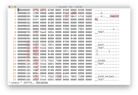
 Here's a quick method I use to edit binary files on the vim editor. Suppose that the binary file name that we need to edit is called hello. Let's open it using the xxd hex viewer utility and pipe it to the vim editor as follows using the terminal. This produces the hex view of the binary file on the vim editor.

xxd hello | vim -

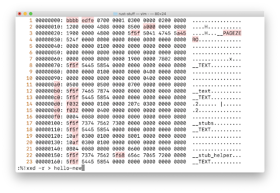
Now, we are good to go with editing the hex values in the file as you would do with any text file on the vim editor. Once we are done with the editing, we can now convert this updated hexdump view on the vim editor back to a new binary file. In order to do that, go to the command mode of the vim editor, and type and enter the following command. It will save the edited binary into a new file; the new file can be named anything while I have made it to be hello-new.

%!xxd -r > hello-new

Now, you can safely quit the vim editor with q! on the command mode as you would always quit it. :) Cheers!

References:

[1] https://vi.stackexchange.com/questions/343/how-to-edit-binary-files-with-vim